 English
 日本語
日本語 한국의
한국의 中文
中文저는 PCB 및 PCBA 설계, 지능형 제어 회로, 생산 최적화 분야에서 10년 이상의 경력을 보유하고 있습니다. 글로벌 엔지니어링 팀과 긴밀히 협력하여 신뢰성, 성능 및 제조 용이성을 개선하고, 복잡한 PCB 기술을 더 쉽게 이해할 수 있도록 실질적인 정보를 공유하는 것을 즐깁니다.

무엇을 찾고 계신가요
?



Author
저는 PCB 및 PCBA 설계, 지능형 제어 회로, 생산 최적화 분야에서 10년 이상의 경력을 보유하고 있습니다. 글로벌 엔지니어링 팀과 긴밀히 협력하여 신뢰성, 성능 및 제조 용이성을 개선하고, 복잡한 PCB 기술을 더 쉽게 이해할 수 있도록 실질적인 정보를 공유하는 것을 즐깁니다.
Engaging professional pcb layout services early in the development cycle bridges the critical gap between theoretical hardware design and practical factory fabrication. In this article, we analyze the 7 most frequent DFM mistakes observed in high-density PCB layouts and provide actionable strategies to eliminate costly engineering change orders (ECOs) and avoid remanufacturing cycles.
1.Trace/Space vs. Copper Weight
The Risk: Specifying clearance on copper causes chemical over-etching or bridging.
DFM Solution: For copper, maintain ; for , keep . Consult our printed circuit board services for fine-pitch BGA tolerances.
2. Via-in-Pad Without Resin Fill
The Risk: Open vias in SMT pads cause solder wicking, leading to voids or open joints under BGAs.
DFM Solution: Specify IPC-4761 Type VII (Via Fill & Cap) in your circuit board design to ensure a flat, solderable pad surface.
3. Acid Traps (Acute Angles)
The Risk: Internal angles < 90 trap etching chemicals, causing long-term copper corrosion.
DFM Solution: Stick to 45 or curved traces and run automated DRC before Gerber export.
4. Solder Mask Slivers & Bleed
The Risk: Mask dams < 4 mil flake off and bridge pads; insufficient clearance covers solderable area.
DFM Solution: Enforce a minimum 3.5-4 mil solder mask damper. Professional pcb design services pre-configure these rules automatically.
5. Annular Ring Breakout
The Risk: Undersized pads lead to hole breakout during mechanical drilling, breaking circuit connectivity.
DFM Solution: Follow IPC-2221 Class 2 ( 2mil copper ring around the hole edge).
6. Solid Plane Connections (Tombstoning)
The Risk: Direct connection to copper planes without thermal relief drains heat unevenly, causing component tombstoning.
DFM Solution: Use 4-spoke thermal relief patterns on all plane connections for pcb custom jobs.
7. Missing Fiducials & Silk Overlap
The Risk: Missing optical marks lowers SMT accuracy; silkscreen on pads ruins solderability.
DFM Solution: Place global/local fiducials and set a 3 mil silkscreen-to-mask clearance.
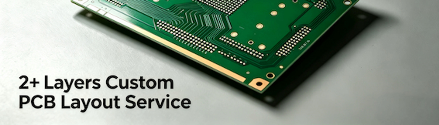
Need end-to-end circuit board design services, fast PCB prototyping, or turnkey PCBA? Ruichun conducts free automated DFM checks before manufacturing.
👉 Upload Gerber for a free quote: www.ruichunpcba.com
메시지를 남겨주세요
스캔해서 WhatsApp으로 전송 :



 IPv6 네트워크 지원